


Available from:
Amazon.com
Manufacturer:
Huafansmart.com
| GPIO # | Component |
|---|---|
| GPIO00 | Led1i |
| GPIO01 | None |
| GPIO02 | None |
| GPIO03 | Led2i |
| GPIO04 | Button1 |
| GPIO05 | Relay1i |
| GPIO09 | None |
| GPIO10 | None |
| GPIO12 | HLWBL CF1 |
| GPIO13 | HLWBL SEL |
| GPIO14 | HLW8012 CF |
| GPIO15 | None |
| GPIO16 | None |
| FLAG | None |
{"NAME":"Huafan SS","GPIO":[56,0,0,57,17,29,0,0,132,130,133,0,0],"FLAG":0,"BASE":24}Introduction
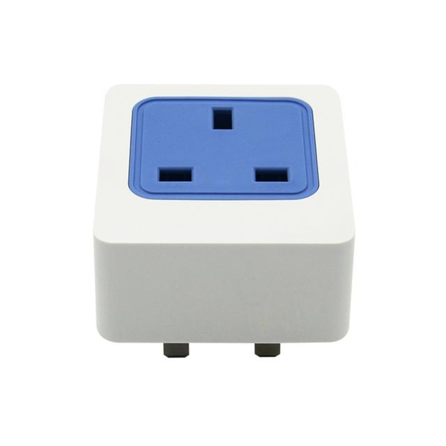
 The HuaFan Wireless Wifi Smart Plug/Socket is a useful bit of kit that allows you to introduce home automation without getting into any mains re-wiring. As an added bonus, the device also provides energy monitoring functions (voltage, current, power) in much the same way as the Sonoff Pow module does.
As you may have guessed, its ‘smarts’ come from an embedded ESP8266, which makes it a potential target for the excellent Tasmota code.
The HuaFan Wireless Wifi Smart Plug/Socket is a useful bit of kit that allows you to introduce home automation without getting into any mains re-wiring. As an added bonus, the device also provides energy monitoring functions (voltage, current, power) in much the same way as the Sonoff Pow module does.
As you may have guessed, its ‘smarts’ come from an embedded ESP8266, which makes it a potential target for the excellent Tasmota code.
This guide provides details on how to prepare the socket for the initial flashing with Tasmota code.
What is it?
 This smart socket comes with its own iPhone/Android App and is controllable from the HF Smart cloud service. As well as allowing on/off control, the plug/socket also measures current, voltage and power. It’s pretty well made but almost certainly doesn’t meet the full British electrical standards, as it doesn’t have a shutter to close off the live socket holes when a plug is removed. This a rather a shame and would not be too tricky to implement and would only marginally increase the cost of these pretty cheap (~£UK 10) units.
The provided software/service all seemed rather closed and proprietary and not able to talk to other stuff. So something had to change!
This smart socket comes with its own iPhone/Android App and is controllable from the HF Smart cloud service. As well as allowing on/off control, the plug/socket also measures current, voltage and power. It’s pretty well made but almost certainly doesn’t meet the full British electrical standards, as it doesn’t have a shutter to close off the live socket holes when a plug is removed. This a rather a shame and would not be too tricky to implement and would only marginally increase the cost of these pretty cheap (~£UK 10) units.
The provided software/service all seemed rather closed and proprietary and not able to talk to other stuff. So something had to change!
Disassembly
WARNING - Opening the unit potentially exposes mains voltages that can kill. You proceed beyond here entirely at your own risk.
 There are no screws; to disassemble you need to prise it open on each side.
Inside there is a main board with most of the components on the reverse. The Wi-Fi and control comes from a small daughter board, soldered to the main board.
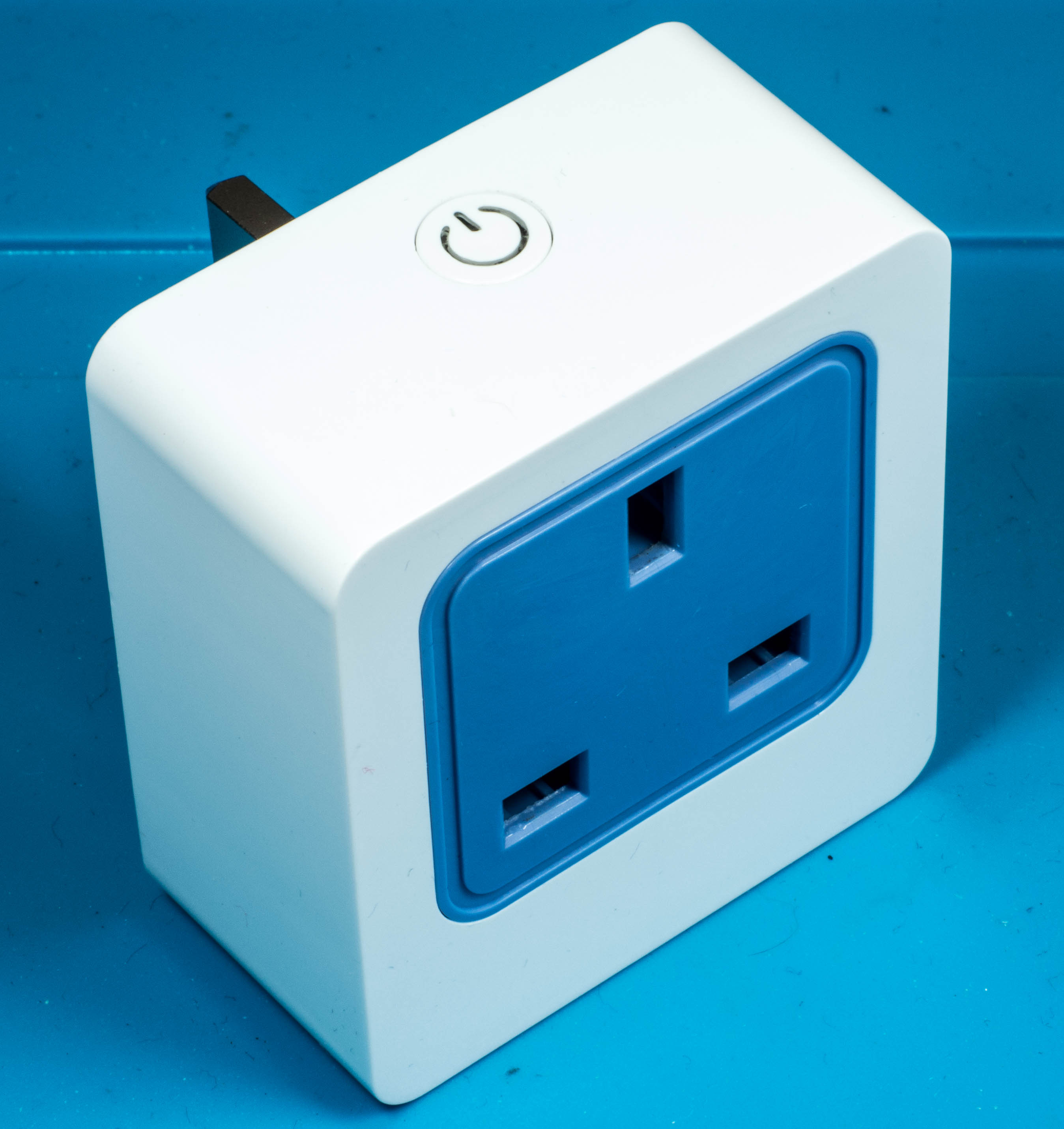
 There’s not a lot to see on the top apart from the mains relay, the button and the red/blue LEDs that illuminate it.
 The main item of interest on the top is the daughter board. This has our trusty ESP8266EX and a 8Mbit SPI flash memory. You can also see the 40MHz crystal - more on this later…

The main item of interest on the top is the daughter board. This has our trusty ESP8266EX and a 8Mbit SPI flash memory. You can also see the 40MHz crystal - more on this later…


The reverse of the daughter board is pretty bare - only the Vcc (3.3V) and GND are marked. In this view you can also see the red and blue LEDs and the push button. In its original configuration the red LED normally is set to the same state as the relay and the blue LED provides information on the state of connectivity.

Another warning…
What is marked as GND IS NOT GROUNDED, it’s not even floating, GND IS CONNECTED TO THE NEUTRAL LINE OF THE MAINS. Do not connect any equipment or yourself to the board whilst it is plugged onto a mains socket - EVEN IF THAT SOCKET APPEARS TO BE SWITCHED OFF. Neutral is not 0V or Ground and should be treated as live (just in case it really is). Always completely disconnect your programming / serial interface before plugging the device into a mains socket.
 You need a hefty soldering iron to unsolder the board from the plug pins and on the reverse you see the main circuitry. Next door to the AMS1117 3.3V regulator for the ESP is a HLW8012 chip that does the current/voltage/power measurement. Conveniently, this is the same chip that’s used in the Sonoff Pow module, so all the code to drive it is already in place. Below the two ICs is R12 it’s R002 i.e. a 2mOhm resistor. This may be different to the one in the Sonoff, so expect to use different calibration settings.
Hookup
Unless you are just curious, there’s no real need to unsolder the main board. You can get at everything you need to re-flash it on the top side of the main board.

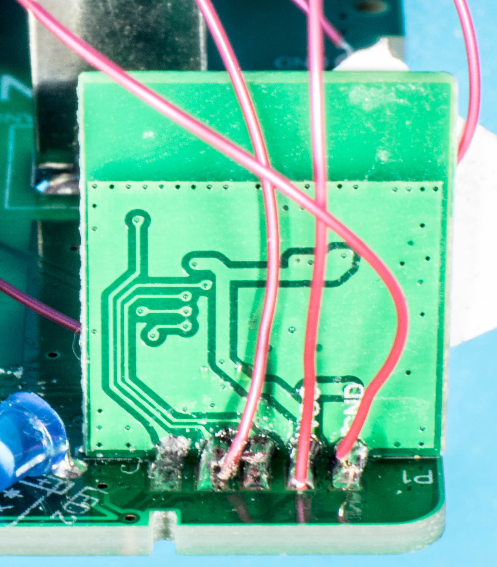 For programming you need to unplug the unit for any mains and make connections to GND, Vcc and Rx. That’s 1, 2 and 4 on the back of the daughter board, counting from the right.
The connection for Tx should have been on the back of the daughter board (all the circuit board tracks are in place on the daughter board). However, for some reason they didn’t populate R5 (or removed it after programming) so the Tx signal does not appear on the rear of the board like it was clearly designed to do.
 Instead you have two options, either re-instate R5 with a very small piece of wire (or a teeny resistor if you have one) or solder a wire directly to the resistor pad/chip pin. As the connection should be temporary (subsequent flashes will be Over the Air) I initially went for the simpler but more fragile direct connection, mechanically secured with some insulating tape.
If you do prefer to solder a small wire across R5 then you will need to cut the small links on the main board around pad 5, as the designers of the main board have connected this pad to the GND plane with two small links, one at the end and to the left side of the pad. Again, all this is on the top of the main board, you don’t need to go delving underneath.
On the front of the daughter board there is the GPIO0 pin (pad number 4, reading from the left). This needs to be manually connected to ground and then the power applied to the ESP8266 to put it in programming mode. You can solder something onto this, as shown, or pick it up where it connects to the blue LED with a small clip probe.

Daughter board pinout
Viewed from above the main board
                         Front     Back
GPIO14 - HLW8012 P pulse     1 |B| 1  0V (marked GND)
GPIO12 - HLW8012 I/V pulse   2 |O| 2  3.3V (marked VCC)
GPIO13 - HLW8012 I/V select  3 |A| 3  GPIO05 - Relay-
GPIO00 - Blue LED-           4 |R| 4  GPIO03 (U0RxD) - Red LED-
GPIO04 - Button-             5 |D| 5  Initially GND but ready for GPIO01 (U0TxD)
Hookup - Solder Free Option
Adding to the great guide above …
So if soldering isn’t your bag, there are a few connection points that you can get at with clip probes. There is a +5V and GND contact on the left side of the board and the right LED legs give access to the ESP’s GPIO0 and RXD. The tricky bit is the ESP’s TXD line which, as stated before, is only accessible on the daughter board via the chip’s pin or an smd pad above and to the right. @jwrw, I am in awe of anyone that can solder onto this pad! As an alternative, try connecting an alligator clip to a sewing pin 8) to make a probe and holding it in place with your finger during firmware programming (hey, it only has to work once as from then on you use OTA). Powering via the pcb contacts requires more current than my FTDI was able to source so a seperate 5V power supply is required (a Raspberry Pi can provide the +5V/GND via it’s GPIO header if you haven’t got a dedicated power supply at hand).
